- 您现在的位置:买卖IC网 > Sheet目录473 > MAX2821ETM+T (Maxim Integrated)IC TXRX 802.11B 2.4GHZ 48-TQFN
2.4GHz 802.11b Zero-IF Transceivers
ABSOLUTE MAXIMUM RATINGS
V CC Pins to GND ...................................................-0.3V to +4.2V
RF Inputs: RX_RFP, RX_RFN to GND.........-0.3V to (V CC + 0.3V)
RF Outputs: TX_RFP, TX_RFN to GND..................-0.3V to +4.2V
Baseband Inputs: TX_BBIP, TX_BBIN, TX_BBQP,
TX_BBQN to GND ...................................-0.3V to (V CC + 0.3V)
Baseband Outputs: RX_BBIP, RX_BBIN, RX_BBQP,
RX_BBQN to GND ...................................-0.3V to (V CC + 0.3V)
Analog Inputs: RX_AGC, TX_GC, TUNE, ROSCN,
ROSCP to GND .......................................-0.3V to (V CC + 0.3V)
Analog Outputs: PA_BIAS, CP_OUT, VREF
to GND.....................................................-0.3V to (V CC + 0.3V)
Digital Inputs: RX_ON, TX_ON, SHDNB, CSB, SCLK,
DIN, RF_GAIN, RX_1K to GND................-0.3V to (V CC + 0.3V)
Bias Voltages: RBIAS, BYP ..................................+0.9V to +1.5V
Short-Circuit Duration Digital Outputs: DOUT, RX_DET .........10s
RF Input Power: RX_RFN, RX_RFP.................................+10dBm
Continuous Power Dissipation (T A = +70 ° C)
48-Lead QFN (derate 27.0mW/ ° C above +70 ° C)...........2162mW
48-Lead Thin QFN (derate 38.5mW/ ° C
above +70 ° C) ...................................................................3077mW
Operating Temperature Range ...........................-40 ° C to +85 ° C
Junction Temperature ......................................................+150 ° C
Storage Temperature Range .............................-65 ° C to +160 ° C
Lead Temperature (soldering, 10s) .................................+300 ° C
Stresses beyond those listed under “Absolute Maximum Ratings” may cause permanent damage to the device. These are stress ratings only, and functional
operation of the device at these or any other conditions beyond those indicated in the operational sections of the specifications is not implied. Exposure to
absolute maximum rating conditions for extended periods may affect device reliability.
CAUTION! ESD SENSITIVE DEVICE
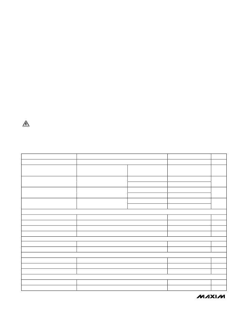
DC ELECTRICAL CHARACTERISTICS
(MAX2820/MAX2821 EV kit: V CC = +2.7V to +3.6V, RF_GAIN = V IH , 0V ≤ V TX_GC ≤ +2.0V, 0V ≤ V RX_AGC ≤ +2.0V, RBIAS = 12k ? , no
input signals at RF and baseband inputs, all RF inputs and outputs terminated into 50 ? , receiver baseband outputs are open, trans-
mitter baseband inputs biased at +1.2V, registers set to default power-up settings, T A = -40 ° C to +85 ° C, unless otherwise noted.
Typical values are at V CC = +2.7V, T A = +25 ° C, unless otherwise noted.) (Note 1)
PARAMETERS
Supply Voltage
CONDITIONS
MIN
2.7
TYP
MAX
3.6
UNITS
V
Shutdown-Mode Supply Current
(MAX2821 and MAX2821A)
Standby-Mode Supply Current
Receive-Mode Supply Current
Transmit-Mode Supply Current
SHDNB = V IL , RX_ON = V IL ,
TX_ON = V IL
SHDNB = V IH , RX_ON = V IL ,
TX_ON = V IL
SHDNB = V IH , RX_ON = V IH ,
TX_ON = V IL
SHDNB = V IH , RX_ON = V IL ,
TX_ON = V IH
T A = -40 ° C to +85 ° C
T A = +25 ° C
T A = -40 ° C to +85 ° C
T A = +25 ° C
T A = -40 ° C to +85 ° C
T A = +25 ° C
T A = -40 ° C to +85 ° C
2
25
80
70
50
35
40
100
110
85
90
μA
mA
mA
mA
LOGIC INPUTS: SHDNB, RX_ON, TX_ON, SCLK, DIN, CSB, RF_GAIN
Digital Input Voltage High (V IH )
Digital Input Voltage Low (V IL )
V CC - 0.5
0.5
V
V
Digital Input Current High (I IH )
Digital Input Current Low (I IL )
-5
-5
+5
+5
μA
μA
LOGIC OUTPUTS: DOUT, RX_DET
Digital Output Voltage High (V OH )
Digital Output Voltage Low (V OL )
Sourcing 100μA
Sinking 100μA
V CC - 0.5
0.5
V
V
RX BASEBAND I/O
RX_AGC Input Resistance
RX I/Q Common-Mode Voltage
RX I/Q Output DC Offsets
0V ≤ V RX_AGC ≤ +2.0V
50
1.25
15
k ?
V
mV
VOLTAGE REFERENCE (MAX2821/MAX2821A)
Reference Voltage Output
T A = -40 ° C to +85 ° C, I LOAD = ±2mA
1.1
1.2
1.3
V
Output Impedance
25
?
2
_______________________________________________________________________________________
发布紧急采购,3分钟左右您将得到回复。
相关PDF资料
MAX2829EVKIT
EVAL KIT MAX2828, MAX2829
MAX2830EVKIT+
KIT EVAL FOR MAX2830
MAX2831EVKIT+
KIT EVAL FOR MAX2831
MAX2837EVKIT+
KIT EVAL FOR MAX2837
MAX2838EVKIT+
KIT EVAL FOR MAX2838
MAX2839ASEVKIT+
KIT EVAL FOR MAX2839A WLP
MAX2839EVKIT+
KIT EVAL FOR MAX2839
MAX2851ITK+
TRANSMITTER MIMO 5GHZ 5CH 68TQFN
相关代理商/技术参数
MAX2821ETM+TD
功能描述:射频接收器
RoHS:否 制造商:Skyworks Solutions, Inc. 类型:GPS Receiver 封装 / 箱体:QFN-24 工作频率:4.092 MHz 工作电源电压:3.3 V 封装:Reel
MAX2821ETM-D
功能描述:射频接收器
RoHS:否 制造商:Skyworks Solutions, Inc. 类型:GPS Receiver 封装 / 箱体:QFN-24 工作频率:4.092 MHz 工作电源电压:3.3 V 封装:Reel
MAX2821ETM-T
功能描述:射频接收器
RoHS:否 制造商:Skyworks Solutions, Inc. 类型:GPS Receiver 封装 / 箱体:QFN-24 工作频率:4.092 MHz 工作电源电压:3.3 V 封装:Reel
MAX2821ETM-TD
功能描述:射频接收器
RoHS:否 制造商:Skyworks Solutions, Inc. 类型:GPS Receiver 封装 / 箱体:QFN-24 工作频率:4.092 MHz 工作电源电压:3.3 V 封装:Reel
MAX2821EVKIT
功能描述:射频接收器
RoHS:否 制造商:Skyworks Solutions, Inc. 类型:GPS Receiver 封装 / 箱体:QFN-24 工作频率:4.092 MHz 工作电源电压:3.3 V 封装:Reel
MAX2822EGM
制造商:Rochester Electronics LLC 功能描述: 制造商:Maxim Integrated Products 功能描述:
MAX2822EGM-D
功能描述:射频收发器 RoHS:否 制造商:Atmel 频率范围:2322 MHz to 2527 MHz 最大数据速率:2000 Kbps 调制格式:OQPSK 输出功率:4 dBm 类型: 工作电源电压:1.8 V to 3.6 V 最大工作温度:+ 85 C 接口类型:SPI 封装 / 箱体:QFN-32 封装:Tray
MAX2822EGM-TD
功能描述:射频收发器 RoHS:否 制造商:Atmel 频率范围:2322 MHz to 2527 MHz 最大数据速率:2000 Kbps 调制格式:OQPSK 输出功率:4 dBm 类型: 工作电源电压:1.8 V to 3.6 V 最大工作温度:+ 85 C 接口类型:SPI 封装 / 箱体:QFN-32 封装:Tray
